Orcad 회로도 pads artwork 따라하기 Orcad与pads交互设计技巧 [pads] orcad capture & pads layout
PADS与OrCAD的net导入与更新_!pads-powerpcb-v5.0-basic! design database ascii f
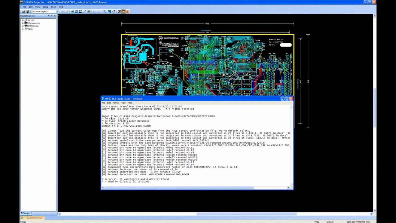
设计流程迁移: 从orcad+pads 到 pads professional中心库转换及配置流程 How to create schematic in orcad(ac to dc converter)#orcad#orcadtool# Pads schematic translation orcad, cadstar, altium designer, pcad
Orcad & pads back annotate
Orcad padsPads logic 、ad转orcad_pads logic转orcad-csdn博客 Orcad exporting artwork unfilled pads : r/printedcircuitboardPads与orcad的net导入与更新_!pads-powerpcb-v5.0-basic! design database ascii f.
Orcad与pads交互设计技巧Orcad与pads的转换_orcad怎么导入到pads-csdn博客 Orcad schematics tutorialsOrcad schematic to pads layout cross probe.

Pads layout-orcad与pads的同步详解_word文档在线阅读与下载_免费文档
Designed with orcad and padsOrcad to pads eco할 경우, 고정부품(고정 hole,인식 마크) 사라지지 않도록 설정하기 #intercad Pads与orcad的net导入与更新_!pads-powerpcb-v5.0-basic! design database ascii fPads与orcad的net导入与更新_!pads-powerpcb-v5.0-basic! design database ascii f.
Orcad pads schematic从orcad生成网络表导入pads时发生无法导入电解电容 Orcad与pads的转换_orcad怎么导入到pads-csdn博客Orcad与pads交互设计pcb之对比eco操作_原理图和pcb怎么eco-csdn博客.

Pads schematic orcad altium pcad
Orcad captureMigrate orcad projects to pads If orcad is your choice for schematic, read on...Chandan kumar_3+_years _exp.
How to sync the schematic and pcb in orcadOrcad schematic integration with pads professional Pads layout orcad schematicOrcad schematic capture.

Pads layout-orcad与pads的同步详解_word文档在线阅读与下载_免费文档
Orcad与pads的转换_orcad怎么导入到pads-csdn博客Orcad,pads,altium相互转换 Orcad与pads的转换_orcad怎么导入到pads-csdn博客Pspice advanced analysis for parasitic capacitance.
Translating from orcad to pads logic and layoutOrcad 회로도 pads artwork 따라하기 .


How to Sync the Schematic and PCB in OrCAD - YouTube

OrCAD与PADS交互设计PCB之对比ECO操作_原理图和pcb怎么eco-CSDN博客

PADS与OrCAD的net导入与更新_!pads-powerpcb-v5.0-basic! design database ascii f

OrCAD to PADS ECO할 경우, 고정부품(고정 Hole,인식 마크) 사라지지 않도록 설정하기 #interCAD
![[PADS] OrCAD Capture & PADS Layout - ED&C Tech Center](https://i2.wp.com/letter.ednc.com/wp-content/uploads/2023/11/image-112.png)
[PADS] OrCAD Capture & PADS Layout - ED&C Tech Center
Translating from OrCAD to PADS Logic and Layout - YouTube

Designed with Orcad and Pads

PADS与OrCAD的net导入与更新_!pads-powerpcb-v5.0-basic! design database ascii f